Market Leader
Thick Film Printing
on Ceramic Substrates:
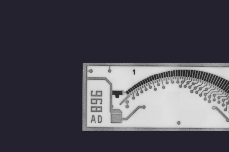
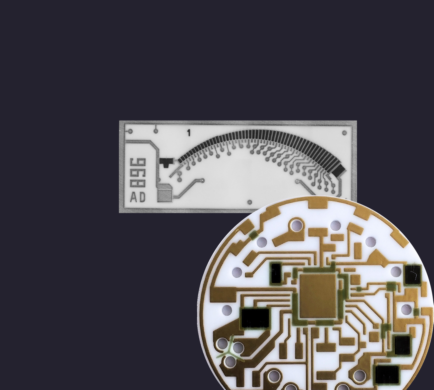
C-MAC is one of the pioneers in thick film technology and market leader today with an unparalleled experience and capacity to provide all ceramic circuit solutions you might need.
Thick film technology means: high reliability, high stability under extreme temperature and moisture conditions, excellent power handling. These features make this the circuit of choice for many sensor & power applications. Also heaters profit from Thickfilm technology due to it’s uniform surface temperature, high thermal conductivity, fast heating and fast cool down & precise controlled electrical properties. A Thick Film ceramic circuit provides the ability to combine analog, digital & power on a single substrate. Our capacity grew the last 3 years further to included several printing lines capable of printing high volumes in different sizes.
+50 years
Experience:
Providing electronics circuits with guaranteed superior performance, stable under extreme temperature, power & heat conditions
Leading Process
Capabilities:
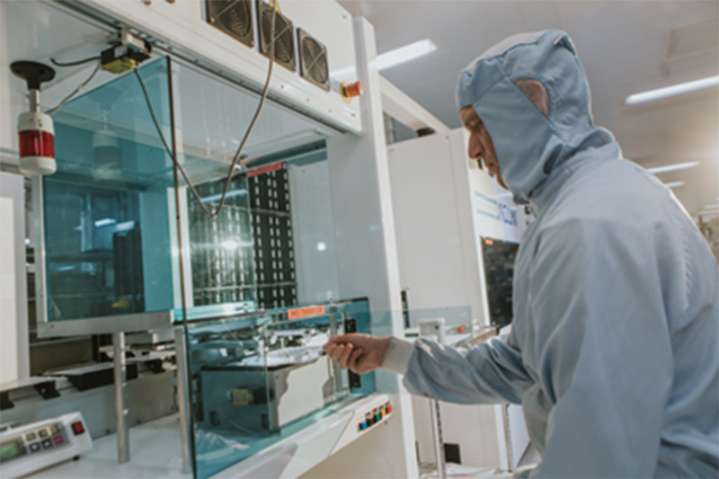
Clean room with 10+ Printing lines, various type of trimmers, unique automated singulation extensive AOI capabilities
Supply Chain
Management
Extensive supplier relations, Competitive & Reliable, Experience with VMI, KANBAN, JIT and flexible to adapt to specific customer needs
Our solution engineers are here to help
Navigating challenges, delivering solutions


Frequently
Asked
Questions
The standard dimensions are 4×4, 4×6 and 5×6 inch. Other dimensions, up to 12 inch, can be handled. The standard thickness is 0.025” (0.635mm) or 0.040” (1.016mm) but can vary between 0.25 and 2 mm. Rectangular shapes are the standard, but any shape is possible thanks to laser profiling. Standard dimensions are the best economical choice.
The standard ceramic substrate is 96% Al2O3 (alumina)
The printed ceramic substrates can be populated on standard SMT lines. They are also ideal for chip-on-board technology
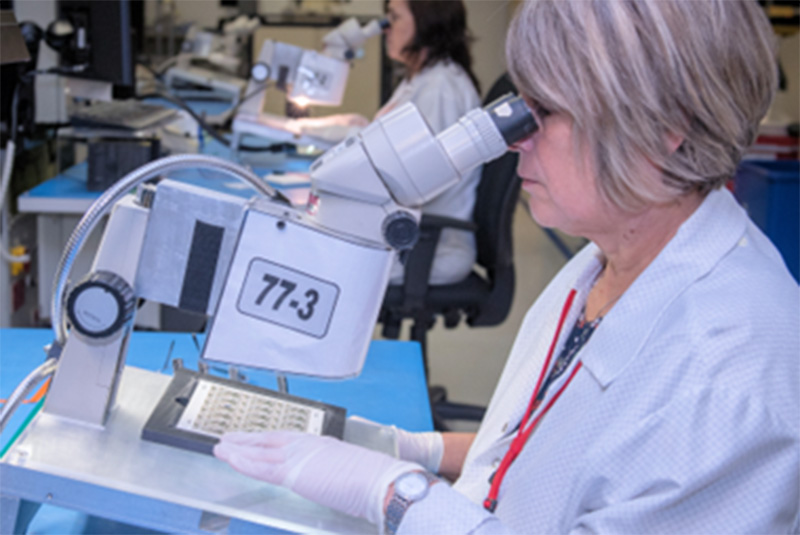
Several printing lines incorporate AOI of the printed wet paste. There is also AOI on the finished part and electrical measurements (continuity check, short circuit check, high voltage breakdown test for multilayers, resistivity).
Printing of multiple layers on the 2 sides is standard. Connection between top and bottom side is realised with metallized through hole technology.
Various options from top suppliers including conductive, resistive & insulating inks. The conductive inks are based on Au or Ag with addition of Pd and/or Pt to improve specific characteristics.
Resistors of any value, tolerance (down to 0,1%), power rating can be integrated. The stability and reliability is outstanding. Printed resistors can also serve as heating element.
Automotive: IATF16949; Medical: ISO-13485; Aerospace: EN 9100


